
Prober Shuttle PS8e
A compact, fully integrated nanoprobing system — now encoded for automatic probe pre-alignment. Optimized for the 3 nm node and beyond.
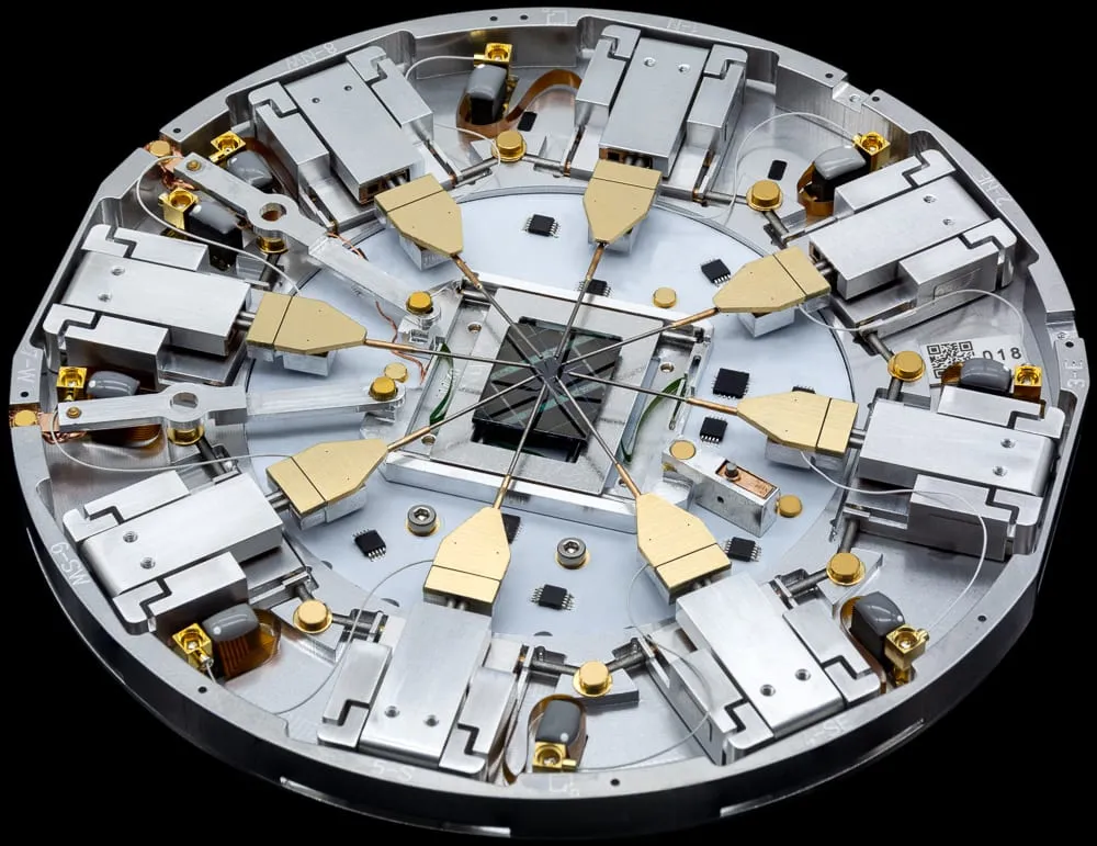
Encoded on all 27 axes#
The PS8e is the encoded evolution of Kleindiek’s 140 mm Prober Shuttle platform. Every one of its 27 axes of motion (the three axes on up to eight ultra-flat MM4 manipulators, plus the three-axis substage) now incorporates a positional encoder, so the system always knows exactly where each probes and the sample sit. A full park-and-restore cycle across all eight probes and the substage completes in about one minute, and a list of user-definable store points lets you re-address the same sample locations on demand instead of spending valuable time hunting for them over and over again.
Low-kV, start to finish#
The automation is what moves the enables nanoprobing on 3 nm and beyond using the PS8e. Manually locating and landing eight probes requires acceleration voltages high enough to actually see the tips without distortion — voltages that also damage the device you’re trying to characterize. Encoded pre-alignment removes that trade-off: the complete probing workflow, from initial park to the final I–V sweep, runs at low beam energy, so beam-induced damage to the sample is mimimized.
The shuttle pairs with the Advanced Probing Tools suite, including the Live Contact Tester and Electron-Beam-Induced-Current (EBIC/EBAC) imaging modules.
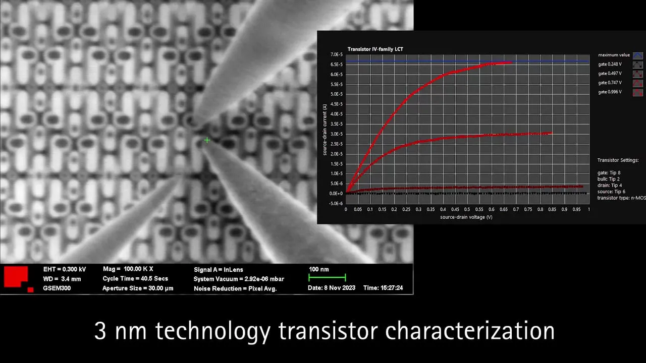
Built for the most advanced nodes#
Noise of just 20 fA at 1 Hz and sub-0.02 nm linear resolution on every axis keep the PS8e suitable for the small currents native to advanced-node devices. Stand-alone electronics sit in a 19-inch rack outside the chamber and out of the operator’s sightline, with the entire system controlled from the APT UI over clean cabling from flange to rack. Non-magnetic and lightweight, the platform drops into your existing SEM or FIB/SEM and tilts to the FIB angle for circuit-edit and delayering work.
Gallery
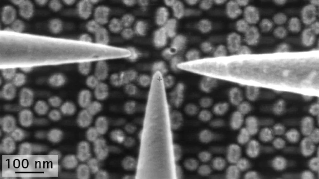
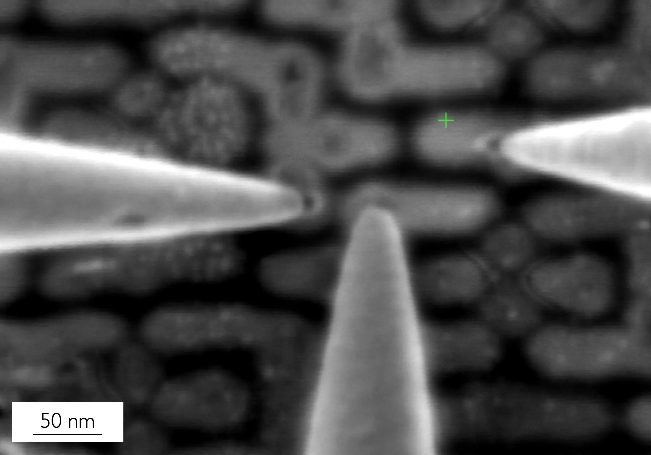
Three probes in contact with the sample — 100 nm scale bar. 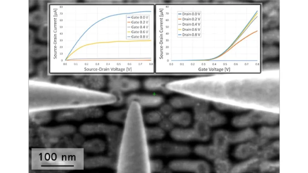
Transistor characteristics acquired on-chip with the PS8e.
Technical data
Overview
- Diameter
- 140 mm
- Total height
- 10 mm
- Max. sample area
- approx. 20 × 20 mm
- Max. sample height
- 20 mm
- Weight
- 200 g + SEM/FIB dovetail
- Manipulators
- up to 8 × MM4
- Encoded axes
- 27 (all)
Substage
- Travel — X / Y
- 9 mm
- Travel — Z
- 0.7 mm
Motion (per manipulator)
- Range — A (left/right)
- 5 mm
- Range — B (rotation)
- 90°
- Range — C (in/out)
- 5 mm
- Resolution — A / C
- < 0.02 nm
- Resolution — B
- < 0.5 nm
- Max. velocity
- up to 1 mm/s
- Drift
- < 1 nm/min
Electrical
- Max. voltage
- 100 V
- Max. current
- 100 mA
- Noise
- 20 fA @ 1 Hz
- Insulation leakage — probes
- < 50 fA/V
- Insulation leakage — sample
- < 150 fA/V
- Signal conductor resistance
- < 5 Ω
See it run
Advantages
Encoded & automatic
- Positional encoders on all 27 axes, so the system always knows where every probe (and the sample) sits
- Park and restore all eight probes and the substage in about one minute
- User-definable store points for repeatable, re-addressable sample locations
Rated for the leading edge
- Complete probing workflow runs at low acceleration voltage, minimizing beam-induced damage to the device under test
- Rated for the 3 nm node and beyond
- Sub-0.02 nm linear resolution and 20 fA noise at 1 Hz keep advanced-node signals readable
Fast & flexible
- Every manipulator's Z drive swings up 90° for direct sample access and easy tip changes
- Non-magnetic design for use with immersion lenses
- Tilts to FIB angle for circuit-edit and delayering work
Easy to integrate
- Plug-and-play, modular components on a lightweight, retrofit-ready platform
- Load-lock compatible; high sample throughput
- Electronics rack stays outside the operator's sightline; controlled entirely from the APT UI, with clean cable management from flange to rack
Application articles
What is nanoprobing?
How in-situ probing measures the electrical behaviour of individual transistors at the most advanced nodes.
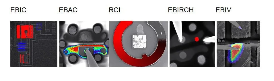
Current imaging for failure analysis
Electron-beam current-imaging techniques that localize faults before you probe.
Nanoprobing in the microscope
In-situ nanoprobing and failure analysis, filmed inside the SEM, from probe landing to live I–V curves.
Related products & accessories
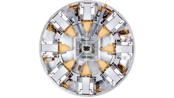
Prober Shuttle PS8
High-precision in-situ electrical nanoprobing with up to eight ultra-flat MM4 manipulators — for advanced-node failure analysis.
View product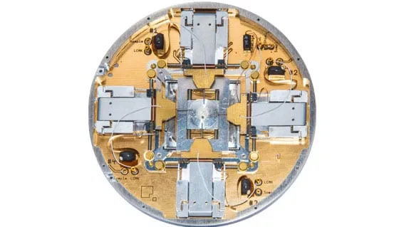
Prober Shuttle PS4
A compact two- or four-probe nanoprobing system for in-situ electrical characterization at advanced nodes.
View productTalk to an application engineer
Tell us your sample and your microscope — we’ll walk you through the workflow and route you to the right regional team.